Extreme care is required where EEE (electrical, electronical and electromechanical) components are to be used for applications in space. Damage to the parts and contamination by foreign materials must be avoided. To use solder in the components is therefore not an option. This is a major challenge, especially where the components to be tested work in the high frequency and microwave frequency range: at these frequencies the cables, adapters and testing fixtures can suffer from parisitic effects. It is therefore extremely important to design test equipment correctly and to compensate for disturbances.
Alter Technology’s (ATN) laboratories in Spain specialise in this type of research. Manufacturers therefore make use of the extensive know-how of ATN’s specialists. “Our laboratories are excellently equipped and prepared to deal with unusual problems," says Aintzane Lujambio, who is responsible for testing EEE components at ATN. Two years ago, the laboratory was significantly expanded and brought up to date with the latest technical standards.
Aintzane Lujambio studied telecommunications engineering at the Public University of Navarre in Pamplona (Spain) and specialised in microwave engineering during her Master’s and Ph.D studies in the Microwave Component Group of the same university. Since 2010, she has been involved in research activities focused on microwave component design and testing. In 2014, she moved to Seville and continued her research activities with the Microwave Group of the University of Seville. In July 2017, she joined ATN to perform tests of radiofrequency and microwave components for space applications.
If dies are inspected, all parasitic effects are removed by using a probe station, explains Aintzane Lujambio. This equipment is basically a high-precision positioning system that uses multiple high-frequency and DC probes to directly contact the connections on the die. Any inaccuracies in the test equipment, the cables and probes themselves are corrected by calibration with appropriate calibration standards prior to electrical measurement. However, this calibration cannot eliminate the effects of environmental conditions. For example, the light spot of a lens used to position the probes can increase the power consumption of some chips. Hence, the entire setup and its environment must be controlled during the measurement process.
“The size of components varies a lot depending on the type of component, but dies are really small”, explains Aintzane Lujambio. The sides of a die may be one millimeter long, or even less, and 0.1 mm thick. This implies that the pads where the probes must be landed may be squares with sides measuring 100 μm. The typical pitch between the contacts of a radiofrequency ground-signal-ground probe is 150 or 200 μm. “That’s why binoculars are necessary to properly place the probes on the die pads. Encapsulated components are bigger and may be placed into the sockets without using binoculars.”
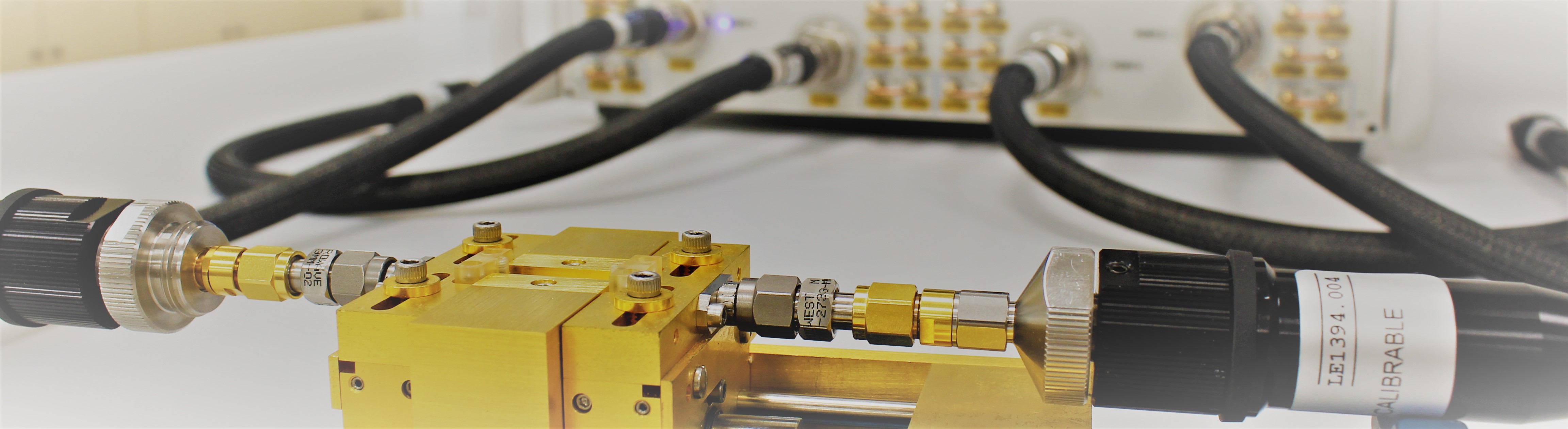
These already encapsulated components need other fixing options. Usually, two alternatives are used: test sockets and customer-specific test fixtures. Sockets for integrated circuits are the most common solution for the testing of analogue and digital components. “In the case of high-frequency and microwave devices, we prefer customer-specific testing devices," explains Aintzane Lujambio.
Sockets allocate the component and contact the printed circuit boards used for the measurements. At microwave frequencies, however, the socket pins produce parasitic inductive and capacitive effects, which can lead to a mismatch of signals and increased insertion losses. High-frequency sockets must be used that are specifically designed to minimise these effects, which increases the cost of the test setup. In any case, the measurement data need to be de-embedded for a precise characterisation of the component. This is a mathematical correction of measurement results that virtually suppresses the parasitic effects of measuring devices and cables. For this purpose, the test setup must be analysed and modelled electromagnetically before the actual test.
An alternative is offered by customer-specific test fixtures which have been developed for the purpose of testing a component. In such test fixtures, the component is placed directly onto the circuit board to improve the electrical contacts. The pressure of the tool is calibrated to prevent damage to the component. The fixture is designed with 3D CAD tools and places special emphasis on commissioning to ensure a good match between connectors and transmission lines. Additional thermal analyses can be carried out on the test fixture to be developed for high performance requirements. The test fixtures are manufactured with precision milling machines. Ad hoc calibration kits have been developed to eliminate the effects of the fixture and to place the reference plane of the measurements on the component.
Finally, any fixing solution is connected to the test and measuring equipment using coaxial connectors and cables. Most electrical measurements are performed using a vector network analyser for S-parameters characterisation. However, other equipment can also be used, such as spectrum analysers, signal source analysers and digital signal analysers. The quality of accessories such as adapters, impedance tuners, attenuators, calibration kits and test cables is very important for accurate and repeatable measurements. For instance, the lack of phase stability of semi-rigid/flexible cables can affect the measured performance.
“There are not many laboratories in the world that can offer the test spectrum at the required depth,” explains Aintzane Lujambio. Nevertheless, the laboratory needs to constantly undergo further development: The components to be tested are becoming more and more powerful and intricate. “We will continue to move forward in that area.”