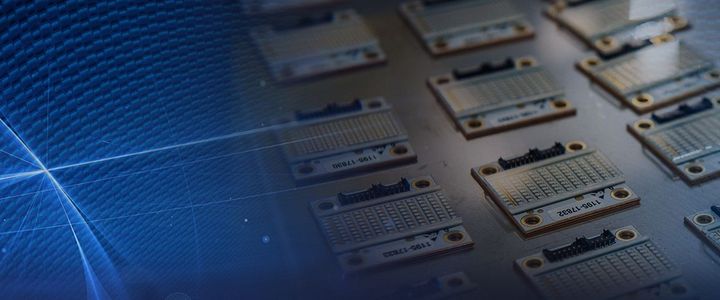
We provide contract package design and precision assembly services for a wide range of optoelectronic, microelectronic and MEMS devices. We offer end to end backend semiconductor manufacturing from wafer singulation to assembled product.
Our process and design IP and know-how enable our customers to reduce development and manufacturing costs, accelerate time to market and reduce risk with any new product development.
Our expertise in semiconductor packaging solutions spans the full product life-cycle: from design through prototyping, process optimisation, product qualification, failure analysis, volume manufacturing and transfer to low-cost volume manufacture.
APPLICATIONS
DESIGN
Understanding the required environmental operating conditions, thermal, optical, mechanical and electrical requirements are the key to any successful package design activity for semiconductor devices. We have extensive design capability in all these areas for a large number of product types and markets.
ASSEMBLY PROCESSES
PRODUCTS
Narrow linewidth lasers are a key enabling technology in application areas as diverse as holography, remote sensing, spectroscopy and quantum technologies. In the quantum technology area alone, these sources are at the heart of atomic clocks, gravitometers and inertial navigation sensors empowered by laser-cooled atoms.
With the launch of the FLAME and REMOTE product lines, we have applied our pedigree in telecoms and space qualified devices to narrow linewidth lasers. This new generation of compact, stable and reliable lasers opens the door to real world applications of narrow linewidth lasers outside of the laboratory environment.
5 Bain Square
Livingston Scotland, UK EH54 7DQ
Tel.: +44(0)1506 403 550
info@uk.altertechnology.com