


Solderless Measurements on Microwave
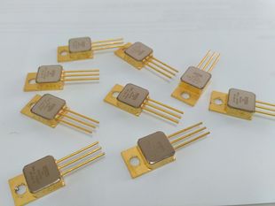
Screening activities for space applications requires extreme care during the manipulation of the EEE parts to be assembled on a spacecraft. This means that special attention shall be paid to avoid damages on the pieces and any contamination of foreign materials. Soldering of the pieces is hence totally forbidden resulting in a big challenge when the components under test operate at radio frequency and microwave frequency ranges. At these operation frequencies, parasitic effects of the cables, adapters, or test fixture become extremely important and must be correctly designed and compensated. When screening is performed at die level, all these problems are solved with the use of a probe station. This equipment is basically a high precision positioning system where several RF and DC probes are used to contact directly the pads on the die. Any inaccuracies on the test equipment, the cables and the probes themselves, are removed through the calibration process performed using adequate calibration standards prior to the electrical measurement. However, this calibration does not remove the effects produced by environmental conditions. For example, the light spot of the binoculars for the positioning of the probes may increase the power consumption of some silicon technologies. Hence, all the setup and its environment need to be controlled during the measurements. If the components are already encapsulated, other fixturing options shall be found. Usually two alternatives are employed: test sockets and customized test fixtures. Integrated circuits sockets are the most common solution when testing analog and digital components. For RF and uW devices the usage of customized test fixture is preferred. Sockets allocate the component and contact the printed circuit boards used for the measurements. However, at microwave frequencies the socket pins present parasitic inductive and capacitive effects that may produce the mismatch of the signals and increased insertion losses. High frequency sockets must be used which are specially designed to minimize these effects which increase the cost of the test setup. Anyhow, for a precise characterization of the component measured data should be de-embedded. De-embedding is the act of taking data that is measured in a test fixture and removing the effects of the fixture so that the data is accurate to reference planes. This requires performing an electromagnetic analysis and modelling process of the test fixture in advance. The alternative to sockets are the customized test fixtures, specifically designed for a specific component together with an ad-hoc calibration kit. In those test fixtures, the component is placed directly on the board as if it would be soldered, but instead it is pressed to improve the electrical contact. The pressure of the tool is calibrated to avoid damages on the component. The fixture is designed with 3D CAD design tools and paying special attention to the launches for a good matching of the connector and the transmission lines. In addition, when high power capability is required, additional thermal analysis may be performed on the test fixture under design. The test fixtures are manufactured with precision milling machines. The ad-hoc calibration kits are designed to remove the effects of the fixture and place the reference plane of the measurements at the component. Any fixturing solution is finally connected through coaxial connectors and cables to the test and measurement equipment. Most electrical measurements are performed using a vector network analyzer for S parameter characterization. However, other equipment may be also used such as spectrum analyzers, signal source analyzers or digital signal analyzers. The quality of the accessories such as adapters, impedance tuners, attenuators, calibration kits or test cables are very important for accurate and repeatable measurements. For instance, lack of phase stability of semi-rigid/flexible cables may affect the measured performance. In Alter Technology, we can perform: • S-parameter characterization up to 50 GHz with the four port N5245A PNA-X network analyzer of Keysight Technologies, the world’s most integrated and flexible microwave test equipment for measuring both passive and active devices. • VCO characterization up to 7 GHz with the E5052B Signal source analyzer which features many enhanced performance characteristics to offer world’s highest measurement throughput and best usability in a single test setup. • Spectrum and harmonic characterization up to 26.5 GHz with the E4407B Spectrum analyzer. Specific options for noise figure and phase noise measurements are included in our device expanding the capabilities of the signal source analyzer. • Time measurements up to 12 GHz with the 4 channel DSO81204B Digital signal analyzer with a sample rate of 40 GSa/s.