Advanced Packaging for Power Electronics
Unlocking higher efficiency through next‑generation GaN-in-PCB integration

Unlocking higher efficiency through next‑generation GaN-in-PCB integration
This project develops a next-generation advanced packaging solution for power electronics by embedding a GaN power device directly inside a multilayer printed circuit board (PCB). This approach minimizes electrical parasitic, specifically stray inductance and stray capacitance, which are primary limitations in high-speed, high-efficiency power conversion systems.
GaN devices are capable of extremely fast switching, but conventional packaging often limits their performance due to long bonding wires and large loop dimensions. Embedded-die PCB technology directly addresses these bottlenecks, shortening current loops, reducing dielectric spacing, and improving thermal and electrical performance. Embedded-die PCB techniques refer to methods for integrating semiconductor dies directly within PCB layers, enabling enhanced electrical and thermal characteristics compared to traditional approaches.
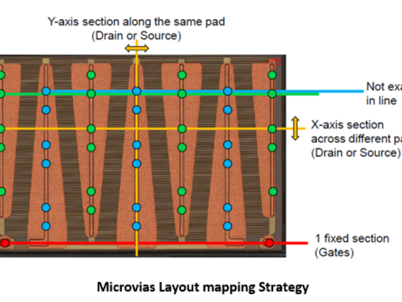
A custom Test Vehicle (TV) was designed with precise interconnect routing and instrumentation to validate the embedded-die concept. Microvias connect the die pads to the copper layers, supporting both low-parasitic performance and monitoring for reliability assessments.
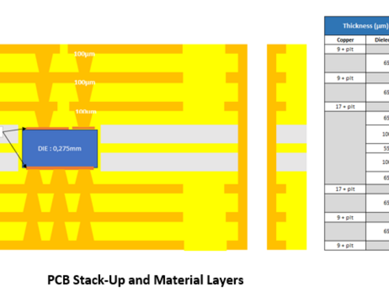
The GaN die (~275 µm thick) is embedded within a 10-layer PCB stack-up, surrounded by Epoxy Molding Compounds (EMC) materials and interconnected through copper microvias. EMC materials provide mechanical protection and electrical insulation for the embedded die. Thick copper planes support high-current paths, while dielectric laminates ensure mechanical and electrical integrity. An interposer, which is a thermal interface component, can be added to extract heat from the PCB and improve thermal management. This embedded-die PCB approach can also be applied to RF modules, optical transceivers, and other high-performance electronic systems where size, efficiency, and reliability are critical. These examples demonstrate the versatility and commercial relevance of technology.

Reliability was evaluated through Thermal Shock Testing (-40°C to 125°C) on 40 samples, alongside electrical and thermal monitoring. Finite Element (FE) models (2D, axisymmetric, and 3D) were developed to simulate thermomechanical stresses. Including manufacturing-induced residual stresses improved lifetime prediction accuracy by approximately 30%.
· Significant reduction of parasitic inductance and capacitance
· Improved switching performance and Electromagnetic Interference (EMI) behavior
· Higher power density
· Improved reliability prediction through advanced FE modeling
· Finalize ongoing thermal shock campaign and correlate results with FE simulations
· Optimize microvia geometry and PCB stack-up for industrialization
· Prepare second-generation test vehicle incorporating design improvements
· Evaluate integration into functional converter demonstrators
Embedded-die PCB packaging represents a strategic breakthrough in power electronics and is not limited to such market. By integrating power die directly into the PCB, we significantly reduce parasitic elements, enhance switching performance, and enable more compact and efficient converter architectures. Beyond power electronics, this technology can be leveraged in RF modules, optical transceivers, and other advanced electronic systems where miniaturization, efficiency, and reliability are essential. The broad applicability of embedded-die PCB techniques positions this innovation as a versatile platform for next-generation electronics across multiple industries.